
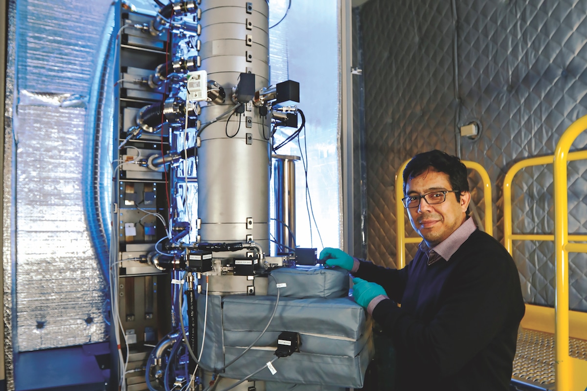
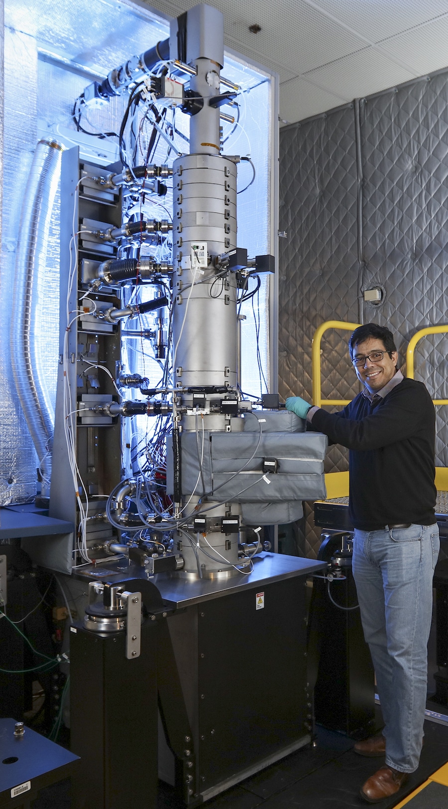
Juan Carlos Idrobo is making big advances in nanotechnology at the Oak Ridge National Laboratory. [Photo: Jason Richards]
Juan Carlos Idrobo, Oak Ridge National Laboratory
A nanometer is one billionth of a meter—think 100,000 times smaller than the width of a human hair. That’s the scale where Juan Carlos Idrobo, a researcher at U.S. Department of Energy’s Oak Ridge National Laboratory in Tennessee, does his research. “Literally, I see where the atoms are, what the atoms are doing,” he says. “That allows me to better understand a material’s properties.” Studying materials on this small scale can lead to big advances in technology.
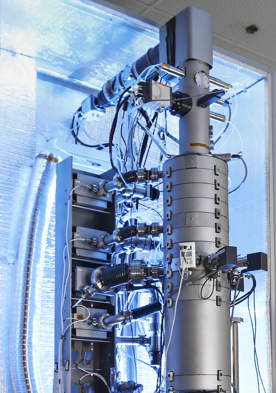
Earlier this year, Idrobo was part of a team that discovered a new way to determine the temperature of a material that’s just a nanometer wide. They did it using something called a high-energy resolution monochromated electron energy-loss spectroscopy-scanning transmission electron microscope—or HERMES, for short.
Why does this matter? The technique could make it possible to observe very slight changes in temperature in very small pieces of material. It will allow researchers to read a material’s temperature as it changes phases. And it works across a wider range of temperatures than other thermometers.
Overall, the technique could help experts develop more efficient building materials by helping them understand how the materials perform on the atomic scale. Idrobo is especially excited about the applications related to transistors, the semiconductor devices that are a critical part of heating and cooling systems.
[Photo: Jason Richards]
gb&d: How would you describe what you do for a living?
Juan Carlos Idrobo: I study materials at the atomic scale using an electron microscope. Basically, I take pictures of atoms and electrons, using the electron microscope as my camera, in order to understand how they control the material’s properties and how these properties can be enhanced.
gb&d: How did you come to pursue research in nanotechnology?
Idrobo: It was little bit of an accident. I was interested in doing a PhD in astrophysics, using telescopes to study the cosmos. But during my PhD classes my interest changed, and instead I began using the electron microscope to study the universe, albeit one atom at a time.
gb&d: Can you walk us through how you use the electron microscope for measuring temperature?
Idrobo: First, let’s think about a thermometer you’re used to, like a mercury thermometer. The way that works is that the mercury is in a cylinder of glass and there are marks on the glass, whether it’s in Celsius or Fahrenheit, for all the measurements—40, 50, 60, 70 degrees. And depending on the temperature in the area, the mercury will expand. The higher the temperature, the more the mercury atoms expand and that causes the mercury to rise up in the glass. And you can calibrate how to correlate that expansion with the temperature marks on the glass. That will tell you the temperature.
When we take temperature with an electron microscope, we do this completely differently. You can think of a scanning transmission electron microscope like this: All the electrons are focused in a really small area, similar to the light of a laser. But instead of the size of a laser, which might be a few millimeters, the size of the electron beam is on the order of an atom. That is basically one tenth of a billion of a meter—100,000 times smaller than the width of a hair. So, very small.
So what we do is we shoot this beam of electrons through a material. There are tons of electrons—millions of electrons per second—we are bombarding this material. And the electrons interact with the atoms in the material. And as they interact with the atoms in the material, the electrons lose energy, but they can also gain energy. The amount of energy they gain depends on the temperature of the material they’re interacting with.
Then the next thing that happens, you can imagine like light going through a prism. When white light passes through a prism, a rainbow of different colors comes out the other side. The same thing happens when the electrons goes through the material. But instead of an optical prism like you’re imagining, we have a magnetic prism. We separate the electrons based on how much energy they have lost. And then we take a reading of how much energy the electrons have lost, and sort them into buckets. It’s like measuring how much purple we have, how much blue we have, how much red, how much yellow, green. We’re able to measure the temperature of the material by measuring how much energy the electrons have gained and lost.
[Photo: Jason Richards]
gb&d: Why is this technique important?
Idrobo: The thing that is most exciting to me is that with this technique, we don’t care about what the material is. In order to use a thermometer with, say, mercury, you need to know what the properties of the mercury are—how much volume the mercury gains when the temperature increases, for instance. With this technique, we don’t care about that. We can just point the laser at the material and tell the temperature.
The second thing is that because it is very small, we can look at very tiny pieces of material and take the temperature of just a very tiny, specific volume of the material.
Another thing we can do is heat up a material, then stop the heating and let the material cool down. When the material is cooling down we can measure the temperature and see how the material responds when it’s cooling down. Why is important? Because we want to know how materials behave when they heat up or when they cool down. Is the material changing? What are the thermo-properties of the material? What are their electronic properties? What’s the strength? So now we can determine all those things by using this technique—and on a very small nanoscale.
gb&d: What influence could this have on green building techniques?
Idrobo: One good example is transistors. Transistors are shrinking all the time. As technology advances, they are getting smaller and smaller and smaller. But as they become smaller there are issues with thermo-management. There are parts of the transistor that get warmer, and how do you measure how hot these parts are?
But even as they become smaller and smaller and smaller, we don’t have a problem measuring the temperature with an electron microscope—our electron probe is tiny. So this will help in advancing those transistors. And that’s really exciting.
gb&d: How will your research impact energy efficiency in the HVACR industry?
Idrobo: Any technological advancement in society is based in a large amount of basic science research, where materials properties are first characterized and clearly understood. The goal of my research is to provide that basic understanding in new materials so that novel devices can be made. This also apply to HVACR systems, where they can present an enhanced performance because they can rely on these new materials.
Read more gb&d In the Lab features.